

The Problem: Reflections Kill High-Speed Signals
When signals travel along PCB traces, they behave as transmission lines. If the trace impedance doesn’t match the driver and receiver impedance, part of the signal reflects back—causing ringing, overshoot, and data errors. At low frequencies this doesn’t matter; at high speeds it’s critical.
Controlled impedance design ensures your traces have consistent, predictable impedance along their entire length, eliminating reflections and preserving signal integrity.
What Is Characteristic Impedance?
Characteristic impedance (Z₀) is the ratio of voltage to current in a signal travelling along a transmission line. It’s determined by the trace geometry and the materials around it—not by the trace length.
The key factors:
- Trace width – wider traces = lower impedance
- Dielectric thickness – distance to reference plane
- Dielectric constant (Dk) – material property of the laminate
- Copper thickness – minor effect, but still matters
A lossless transmission line has purely resistive characteristic impedance. When terminated with a resistor equal to Z₀, the line appears infinitely long to the source—no reflections occur.
Common Impedance Values
| Application | Single-Ended | Differential |
|---|---|---|
| General digital | 50 Ω | 100 Ω |
| USB 2.0 | 45 Ω ±10% | 90 Ω ±10% |
| USB 3.0 | — | 90 Ω ±10% |
| HDMI | — | 100 Ω ±15% |
| PCIe | — | 85 Ω ±15% |
| DDR4 | 40 Ω | 80 Ω |
| Ethernet | — | 100 Ω |
Microstrip vs Stripline
Microstrip (Outer Layers)
A trace on an outer layer with reference plane below. One side faces air (or solder mask), the other faces the dielectric.
Characteristics:
- Easier to manufacture and probe
- Slightly faster propagation than stripline
- More susceptible to EMI (exposed to environment)
- Effective Dk is lower than bulk material (air on one side)
Stripline (Inner Layers)
A trace sandwiched between two reference planes, fully embedded in dielectric material.
Characteristics:
- Better shielding from external noise
- More predictable impedance (uniform dielectric)
- Lower crosstalk between adjacent traces
- Requires inner layer routing
Impedance Calculation
Modern impedance calculators (like Polar Si8000) model dozens of structures including edge-coupled differential pairs, coplanar waveguides, and asymmetric striplines.
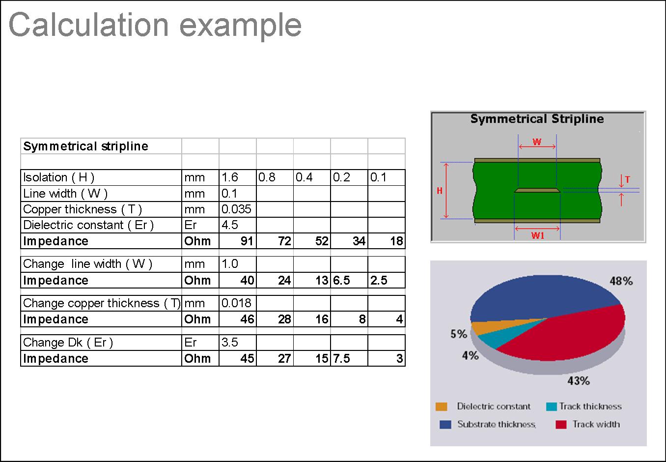
Symmetrical stripline calculation: trace centred between two reference planes
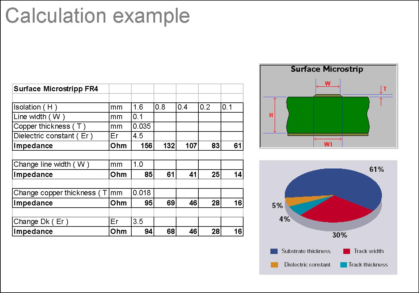
Surface microstrip on FR-4: trace on outer layer with solder mask coating
For calculation tools and application notes, see: Polar Instruments Application Notes
Design Guidelines
Trace Width Tolerances
Impedance depends heavily on trace width. A ±0.5 mil variation can shift impedance by several ohms. Specify your required tolerance—standard is ±10%, tighter tolerances cost more.
Dielectric Thickness
Inner layer dielectric is more tightly controlled than outer layer (where copper plating adds variation). For critical impedances, consider routing on inner layers.
Reference Planes
Every controlled impedance trace needs a solid, uninterrupted reference plane. Breaks in the plane cause impedance discontinuities and EMI problems.
Solder Mask Effect
Solder mask over microstrip traces lowers the effective Dk slightly (typically 0.5–1 Ω effect). We account for this in calculations.
Verification
We calculate impedance as part of our technical review and can verify actual values using Time Domain Reflectometry (TDR) on test coupons included in your panel.
Related Articles
- PCB Materials and Laminates Guide – Dielectric constants for different materials
- Micro-Via Advantages in PCBs – Signal integrity benefits of HDI designs
- Multilayer PCB Capabilities – Manufacturing tolerances for controlled impedance
Need impedance-controlled PCBs? Request a quote – we calculate and verify impedance as part of our technical review.