Embedded Capacitor – Power Planes PCB with-built in capacitance
A reliable capacitor can be formed in a PCB multi-layer board using a composition of dielectric materials. The interconnections of the dielectric material withing the multi-layer PCB package forms embedded capacitance. As a result, this method accommodates frequencies above 1 Ghz. Frequencies that discrete surface mounted capacitors are ineffective at. Furthermore, this method reduces surface mounted components. Therefore offering a smaller final package size.
A capacitance PCB can be built with a thickness below 0.35mm . Using three 50um prepreg layers, two 12 um capacitance dielectrics and 18 um copper foil.
Contact us using our quotation form and ask about embedded capacitance.
Advantages of Embedded PCB Capacitors
- Surface mounted discrete capacitors are ineffective above 1 GHz
- Built in decoupling
- Minimal ESR
- Improved EMI
- PCB embedded capacitors have Low impedance and high capacitance at high frequencies
- Impedance is more critical than capacitance at high frequencies
- Low power bus noise can result in reduced radiated emission
Dielectric material choices
Dupont and 3M offer dielectric laminate. See the below links for datasheets from their respective websites. Contact us to explore how you can effectively incorporate this method into your project.
Embedded capacitance layer in a multi-layer build using blind via’s
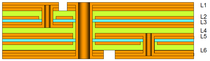
Layer composition for capacitance layer using blind via’s
The list details the layers that appear in the above illustration.
- Final plating 18um
- Second plating 18um
- Base copper 18um
- Core 100um
- Base copper 18um
- Capacitance layer 12um
- Base copper 18um
- Second plating 18um
- Prepreg 100um
- Second plating 18um
- Base copper 18um
- Capacitance layer 12um
- Base copper 18um
- Core 100um
- Base copper 18um
- Second plating 18um
- Final plating 18um
Final PCB thickness: 0.44 mm
Embedded capacitance layer in a multi-layer build without via’s

Simple power plane example:
- A to -12V
- C to +5 V
- B not to any power plane
Layer composition for capacitance layer without via’s
The list details the layers that appear in the above illustration.
- Final plating 18um
- Base copper 18um
- Core 100um
- Base copper 18um
- Capacitance layer 12um
- Base copper 18um
- Prepreg 100um
- Base copper 18um
- Capacitance layer 12um
- Base copper 18um
- Core 100um
- Base copper 18um
- Final plating 18um
Final thickness of this reference board will total up to 0.368mm. Embedded PCB capacitance layers are efficient not only in frequency, but also overall package size.
Contact us using our quotation form and ask about embedded capacitance.