

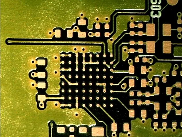
Micro-Via Advantages in Multilayer PCBs
Micro-vias are laser-drilled holes (typically 100–150μm diameter) that connect adjacent layers in HDI PCBs. Unlike mechanically drilled through-holes, micro-vias enable higher density routing and improved electrical performance. Here’s why designers choose micro-via technology.
Key Benefits
Shorter Signal Paths
Micro-vias connect only adjacent layers, eliminating the long vertical stubs created by through-hole vias. This results in:
- Shorter trace lengths – signals travel less distance
- Fewer signal layers needed – more efficient routing in less space
- Better signal integrity – reduced inductance and capacitance
Improved High-Frequency Performance
The shorter signal paths directly benefit RF and high-speed designs:
- Enhanced RF capability – less parasitic inductance
- Improved EMC characteristics – reduced radiation and coupling
- Cleaner impedance control – fewer discontinuities in transmission lines
Higher Component Density
Micro-vias unlock routing options that aren’t possible with through-holes:
- More room for components – via-in-pad allows placement directly under BGAs
- Single-sided assembly becomes viable – avoiding the cost of double-sided placement
- Smaller PCB footprint – same functionality in less board area
For maximum component density, consider the R7011 build which combines buried vias with micro-vias on both surfaces.
Better Reliability
Contrary to early concerns, micro-vias have proven more reliable than through-holes:
- Lower thermal stress – smaller copper volume expands less during reflow
- No barrel cracking – the failure mode that affects long through-holes
- Proven in automotive and aerospace – extensively tested per IPC standards
Additional Advantages
- Embedded passives possible – resistors can be integrated on layers 2 and n-1
- Fewer drilled holes – reduces drilling time and tool wear
- Environmentally friendly – less material waste than mechanical drilling
When to Use Micro-Vias
Micro-via HDI technology makes sense when:
- BGA pitch is 0.8mm or less and fanout requires via-in-pad
- Signal integrity requirements demand controlled impedance with minimal stubs
- Board size is constrained and through-hole routing won’t fit
- High-frequency operation (>1GHz) requires minimal parasitic effects
For simpler designs with larger BGAs (1.0mm+ pitch), standard multilayer builds with blind vias may be more cost-effective.
Micro-Via Examples
BGA fanout example: 64 contacts, 0.8mm pitch, 0.3mm pad, 0.15mm trace/space, 0.3mm vias, 0.1mm micro-vias
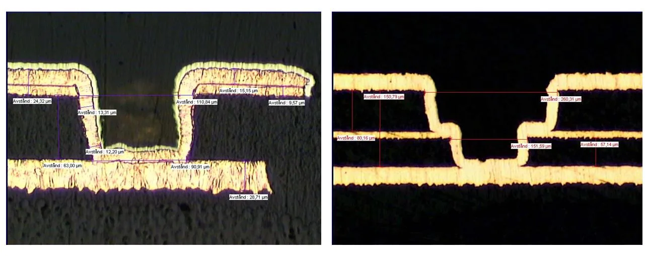
UV laser-drilled micro-via in RCC (resin-coated copper) foil: 0.1mm diameter, stepped 0.2mm to 0.1mm
Learn More
- PCB Build Illustrations – see micro-via stackups R7009–R7020
- Multilayer PCB Stackups – compare HDI vs. standard constructions
- Reliability Testing for Microvias in Printed Wire Boards (PDF) – EIPC conference paper on micro-via reliability
Need help with an HDI design? Our engineers can review your stackup and recommend the most practical micro-via configuration. Get in touch.