Understanding What’s Manufacturable
Before finalising your PCB design, you need to know: can it actually be built? Manufacturing capabilities vary by factory and technology. This reference covers our standard and advanced capabilities—use it to ensure your design is manufacturable and to understand what pushes into premium territory.
Evidence From Supplied Boards
Our production history contains more than 8,000 distinct supplied bare-PCB designs. Within the available manufacturing specifications, we have supplied:
- More than 1,800 high-Tg projects
- More than 500 controlled-impedance projects
- More than 300 projects with blind and/or buried vias
- More than 200 projects with resin-filled via-in-pad
- Heavy-copper builds through 5 oz
These rounded figures are delivered-job observations, not theoretical factory limits. The standard portfolio table below remains 1-40 layers. Material availability and advanced limits vary by construction, so we confirm the complete stackup before production.
Outer and Inner Layer Tolerance Limits
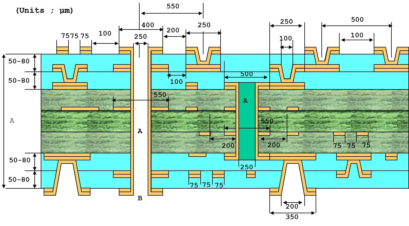
Inner layer clearance: minimum spacing from trace edge to hole wall depends on layer count and hole size
Key dimensions:
- A: For material <0.8 mm, minimum via is 0.2 mm; for thicker material, minimum via is 0.3 mm
- B: Outer layer pads can be landless (no annular ring) in some configurations
Design Rules Check: Inner Layer Clearance Can Be Ambiguous
For inner layers, the design rules check “clearance trace to plated hole edge” is not always interpreted consistently. See the illustration above - the double arrow marks the correct clearance distance of 200 µm. This must be measured from the drill hole edge, not the finished (plated) hole edge.
CAD systems typically work with finished hole sizes. With a 150 µm (6 mil) oversize drill to allow for plating (3 mil each side), a DRC setting of 200 µm will actually pass designs with only 125 µm clearance - which is not safe to manufacture. The setting must be increased by 75 µm to 275 µm total.
Check this before using a new CAD system. Incorrect interpretation of this rule causes significant rework or unusable layouts.
Board Specifications
| Parameter |
Capability |
| Layer count |
1-40 layers |
| Board thickness |
0.13-7.0 mm |
| Maximum board size |
23 × 35 inch (584 × 889 mm) |
| Minimum core thickness |
0.05 mm (standard), 0.13 mm (blind/buried via) |
| Maximum inner layer copper |
10 oz |
| Minimum warpage |
0.10% |
Materials
Standard FR-4
| Material |
Tg |
Notes |
| S1144 |
130°C min |
Standard for 2-layer boards |
| S1141 150 |
145°C min |
Minimum Tg for lead-free multilayer |
| S1155 |
130°C min |
Halogen-free |
| S1165 |
170°C min |
Halogen-free, excellent pad bond strength for repeat soldering |
High-Tg FR-4
FR408, IT180A, PLC-370HR, N4000-13, N4000-13SI
RF/Microwave Materials
Hydrocarbon ceramic: Rogers 4350, Rogers 4003, Arlon 25FR, Arlon 25N
PTFE laminates: Rogers, Taconic, Arlon, Nelco series
PTFE bonding films: RO3001 (1.5 mil), HTI.5 (1.5 mil), Cuclad 6700 (1.5 mil)
PTFE prepregs: Gore Speed Board C (1.5, 2.0, 2.2, 3.4 mil), Taconic TPG-30/32/35 (4.5, 5.0 mil)
HDI Materials
| Material Type |
Specification |
| RCC (Resin Coated Copper) |
12 µm copper, 65 or 100 µm resin |
| LDPP (Laser Drill Prepreg) |
IT-180A 1037 (2.0 mil), IT-180A 1086 (3.0 mil) |
Trace and Space
Inner Layer (Width/Space)
| Copper Weight |
Min Width/Space |
| 1/3-1/2 oz |
3/3 mil (75/75 µm) |
| 1 oz |
3/4 mil (75/100 µm) |
| 2 oz |
5/5 mil (125/125 µm) |
| 3 oz |
6/7 mil (150/175 µm) |
| 4 oz |
7/11 mil (175/275 µm) |
| 5 oz |
10/16 mil (250/400 µm) |
Outer Layer (Width/Space)
| Copper Weight |
Min Width/Space |
| 1/3 oz (12 µm) |
3/3 mil (75/75 µm) |
| 1/2 oz |
3.5/3.5 mil (90/90 µm) |
| 1 oz |
4.5/5 mil (115/125 µm) |
| 2 oz |
6/8 mil (150/200 µm) |
| 3 oz |
8/14 mil (200/350 µm) |
| 4 oz |
10/16 mil (250/400 µm) |
| 5 oz |
12/20 mil (300/500 µm) |
Line Width Tolerance
| Width |
Tolerance |
| < 10 mil |
±1.0 mil |
| ≥ 10 mil |
±1.5 mil |
Holes and Vias
Mechanical Drilling
| Parameter |
Capability |
| Finished hole size range |
0.10-6.5 mm |
| Min hole for PTFE material |
0.25 mm |
| Min blind/buried via |
0.30 mm |
| Min connection hole |
0.35 mm |
| Resin plugging range |
0.10-0.40 mm |
| Hole position tolerance |
±3 mil |
| PTH size tolerance |
±3 mil |
| Press-fit PTH tolerance |
±2 mil |
| NPTH size tolerance |
±2 mil (+0/-2 or +2/-0) |
Laser Drilling (HDI)
| Parameter |
Capability |
| Min laser via (depth < 65 µm) |
0.10 mm |
| Min laser via (depth < 100 µm) |
0.13 mm |
| Blind via for resin fill |
0.075-0.15 mm |
| Blind via for copper fill |
0.075-0.127 mm |
| Min pad size (depth < 65 µm) |
10 mil (0.25 mm) |
| Min pad size (depth < 100 µm) |
11 mil (0.28 mm) |
Aspect Ratio
| Drill Diameter |
Max Board Thickness |
Aspect Ratio |
| 0.10 mm |
0.6 mm |
6:1 |
| 0.15 mm |
1.2 mm |
8:1 |
| > 0.20 mm |
- |
16:1 max |
Resin Plug Hole Size by Board Thickness
| Board Thickness |
Max Hole Size |
| < 1.6 mm |
0.10-0.15 mm |
| < 2.4 mm |
0.20 mm |
| < 2.8 mm |
0.25 mm |
| < 3.2 mm |
0.30 mm |
Backdrill
| Parameter |
Capability |
| Backdrill hole size |
0.5-6.5 mm |
| Stub length (to target layer) |
< 0.20 mm |
| Depth tolerance |
±0.10 mm |
Countersink
| Parameter |
Capability |
| Special drill angles |
82°, 90°, 120° (hole size 0.3-10 mm) |
| Normal drill angles |
130° (3.175 mm), 165° (3.175-6.5 mm) |
| Angle tolerance |
±0.10° |
| Hole size tolerance |
±0.20 mm |
| Depth tolerance |
±0.15 mm |
Pad Sizes
| Application |
Min Pad Size |
| Via (8 mil), 0.5-1 oz copper |
14 mil (0.35 mm) |
| Via (8 mil), 2 oz copper |
20 mil (0.50 mm) |
| Via (8 mil), 3 oz copper |
24 mil (0.60 mm) |
| BGA pads |
7 mil (0.18 mm) |
Pad size tolerance: +5% / -10%
Spacing Requirements
Hole-to-Trace Clearance
| Board Type |
Min Clearance |
| Standard (< 8 layers) |
6 mil |
| Standard (< 14 layers) |
8 mil |
| Standard (< 28 layers) |
9 mil |
| Blind/buried via (2-3 laminations) |
9 mil |
Surface Finish Dependent Spacing
| Finish/Feature |
Min Gap |
| Immersion gold pads |
4 mil |
| Gold fingers |
6 mil |
| HASL pads |
7 mil (10 mil on large copper areas) |
| Legend to pad |
6 mil |
| Peelable solder mask to pad |
16 mil |
| Carbon pads |
15 mil |
Board Edge Clearance
| Feature |
Min Distance |
| Copper to routed edge |
8 mil |
| Inner layer isolation tape |
8 mil min width |
V-Score Clearance (Distance from V-Cut to Copper)
| Board Thickness |
20° |
30° |
45° |
60° |
| < 1.0 mm |
0.30 mm |
0.33 mm |
0.37 mm |
0.42 mm |
| 1.0-1.6 mm |
0.36 mm |
0.40 mm |
0.50 mm |
0.60 mm |
| 1.6-2.4 mm |
0.42 mm |
0.51 mm |
0.64 mm |
0.80 mm |
| 2.5-3.0 mm |
0.47 mm |
0.59 mm |
0.77 mm |
0.97 mm |
Surface Finishes
Lead-Free Options
| Finish |
Thickness |
| HASL lead-free |
2-40 µm (min 0.4 µm on large areas) |
| Flash Gold |
Ni: 2.5-5 µm, Au: > 0.025 µm |
| ENIG |
Ni: 2.5-5 µm, Au: 0.05-0.1 µm |
| Immersion Tin |
≥ 1.0 µm |
| Immersion Silver |
0.1-0.3 µm |
| OSP |
0.2-0.3 µm |
| Hard Gold |
Au: max 2.5 µm |
| ENEPIG (soldering) |
Ni: 3-5 µm, Pd: 0.05-0.1 µm, Au: 0.03-0.05 µm |
| ENEPIG (wire bonding) |
Ni: 3-5 µm, Pd: 0.1-0.15 µm, Au: 0.07-0.15 µm |
Leaded option: HASL (Tin/Lead)
Combination finishes: ENIG+OSP, ENIG+Gold Finger, Flash Gold+Gold Finger, Immersion Silver+Gold Finger, Immersion Tin+Gold Finger
Solder Mask and Legend
| Parameter |
Specification |
| Solder mask thickness (on copper) |
10-18 µm |
| Solder mask thickness (via pads/corners) |
5-8 µm |
| Peelable solder mask thickness |
0.20-0.50 mm |
| Min solder mask bridge (green) |
4 mil |
| Min solder mask bridge (other colors) |
5 mil |
| Min solder mask bridge (2-4 oz copper) |
6 mil |
| Min legend width |
4 mil |
| Min legend height |
23 mil (for 12-18 µm base copper) |
Solder mask colors: Green, Yellow, Black, Blue, Red, White, Matte Green
Legend colors: White, Yellow, Black
Legend marking: Serial number, barcode, QR code (white legend only)
Tolerances
Dimensional
| Parameter |
Tolerance |
| Outline dimension |
±0.1 mm |
| Outline location |
±0.1 mm |
| Slot routing |
±0.15 mm |
| Blind NPTH slot depth |
±0.10 mm |
| Layer-to-layer registration |
< 5 mil |
| Min internal radius |
0.3 mm |
Board Thickness
| Thickness Range |
Tolerance |
| < 1.0 mm |
±0.1 mm |
| > 1.0 mm |
±10% |
| Special (< 2.0 mm) |
±0.1 mm |
| Special (2.1-3.0 mm) |
±0.15 mm |
Impedance
| Target Impedance |
Tolerance |
| < 50 Ω |
±5 Ω |
| ≥ 50 Ω |
±10% (±5% available) |
V-Cut and Panelization
| Parameter |
Specification |
| V-cut angles |
20°, 30°, 45°, 60° |
| Angle tolerance |
±5° |
| Symmetrical tolerance |
±4 mil |
| Remaining thickness tolerance |
±4 mil |
| Outline methods |
Routing, V-cut, tab connecting, stamp holes |
Gold Fingers
| Parameter |
Specification |
| Min gap between fingers |
6 mil |
| Chamfer angle tolerance |
±5° |
| Chamfer thickness tolerance |
±5 mil |
| Parameter |
Specification |
| Layer count |
2-4 layers |
| Thermal conductivity |
1-4 W/mK |
| PCB surface finishes |
HASL, Flash Gold (< 1 oz), ENIG, Immersion Silver, Immersion Tin, OSP, Hard Gold, ENEPIG |
| Metal base finishes |
Cu: Ni+Au plating; Al: Anodic oxidation, hard anodic coating, chemical passivation |
| Technologies |
Pre-bonding, post-bonding, agglomerate, metal core, buried metal |
Electrical Testing
| Parameter |
Specification |
| Max test voltage |
500 V |
| Max test current |
200 mA |
HDI Stackup Options
| Type |
Description |
| 1+n+1 |
Single buildup layer each side |
| 1+1+n+1+1 |
Two buildup layers each side |
| 2+n+2 |
Two buildup layers with buried vias (RCC only, buried via < 0.3 mm) |
Via fill options: Resin fill, copper fill
Production Technologies
Backplane, HDI, blind and buried via, embedded capacitance, embedded resistance, thick copper, backdrill
Flex PCB Capabilities
For flexible circuit specifications, see Flex PCB Capability Limits
Related Articles
Questions about capabilities for your design? Request a quote – we’ll review your requirements and confirm feasibility.