

PCB Build Illustrations
These PCB stackup diagrams show industrially sound, commonly used build methods. Based on decades of manufacturing experience, each construct is tested and proven. For deeper guidance on material selection or PCB manufacturing processes, see our Technical Library.
You can solve routing constraints by increasing build complexity—adding layers, blind/buried vias, or laser micro-vias. However, complex builds with HDI features, flex-rigid constructions, or exotic materials increase cost and lead time. Keep builds symmetric—asymmetric stackups warp during lamination.
Symmetric means: layers added at both sides simultaneously, similar prepreg thicknesses, copper planes of equal weight and area, placed symmetrically about the center. Most examples show 4 or 6 layers, but layer count is rarely a limitation.
The art in PCB layout is fitting complex circuitry into simple builds. All graphics on this page are free to copy for private, educational, or commercial use. Right-click → "Copy image" → paste anywhere. Image size adjusts after pasting.
Each illustration has a unique reference code (R7001–R7024). Use these codes when discussing stackups with manufacturers or searching for specific build types.
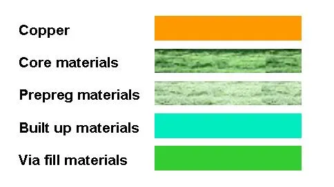
PCB Material Legend – Color key for all stackup diagrams below
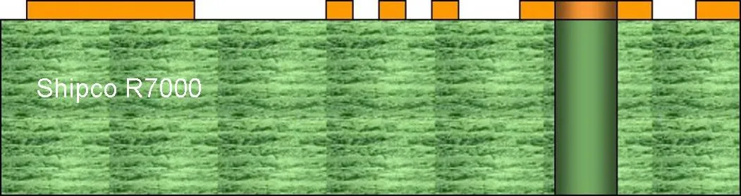
R7000 – Single-sided PCB: copper on one side, through-hole shown for reference
Double-Sided & Multilayer PCB Stackups (R7001–R7008)
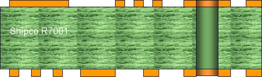
R7001 – Double-sided PCB with non-plated through holes (NPTH)
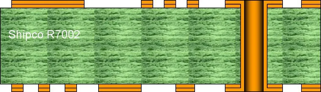
R7002 – Double-sided PCB with plated through holes (PTH)
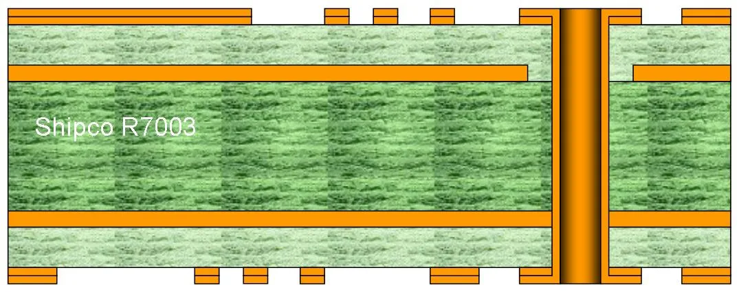
R7003 – 4-layer standard multilayer PCB with through-hole vias
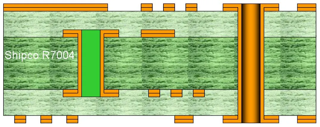
R7004 – 4-layer PCB with buried vias L2–L3 (requires via fill)
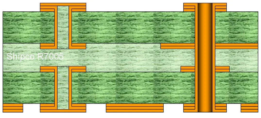
R7005 – 4-layer with mechanically drilled blind vias L1–L2 and L3–L4
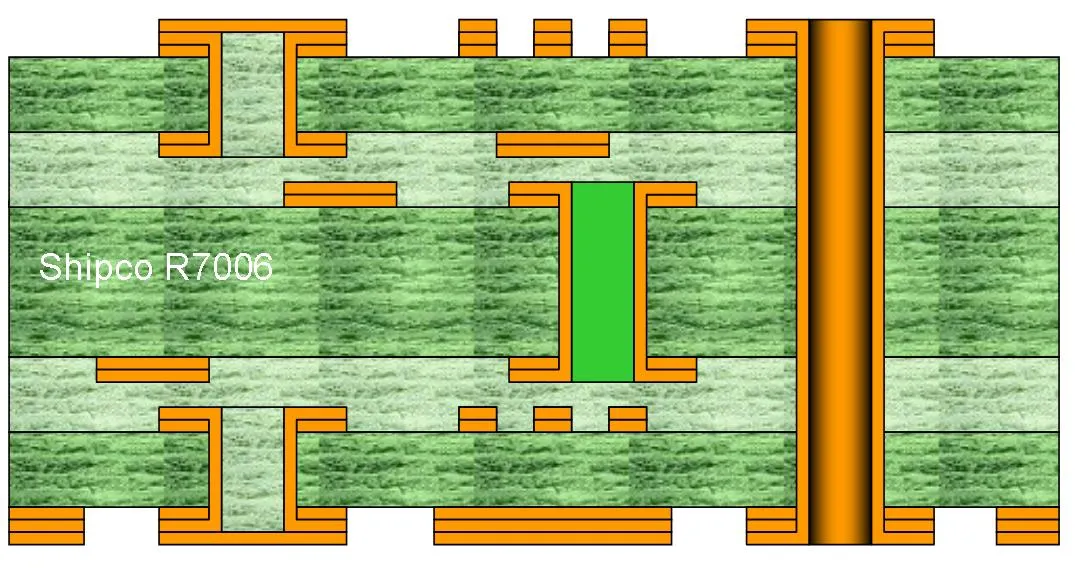
R7006 – 6-layer with buried vias L3–L4 and drilled blind vias L1–L2 and L5–L6
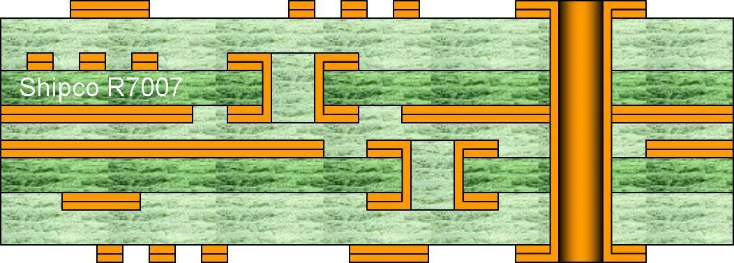
R7007 – 6-layer with two buried via layers: L2–L3 and L4–L5
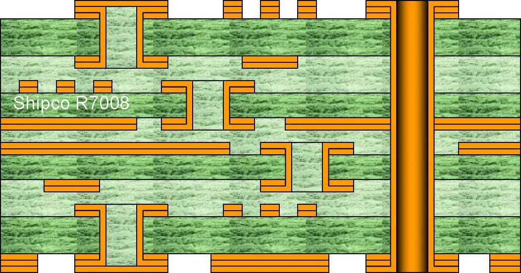
R7008 – 8-layer with buried vias L3–L4 and L5–L6, blind vias L1–L2 and L7–L8
HDI Micro-Via PCB Builds (R7009–R7020)
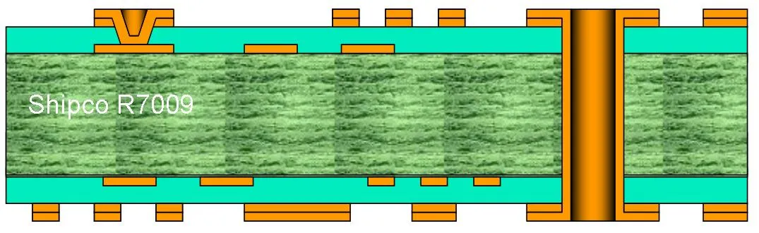
R7009 – 4-layer HDI with laser micro-via on top side only (L1–L2)
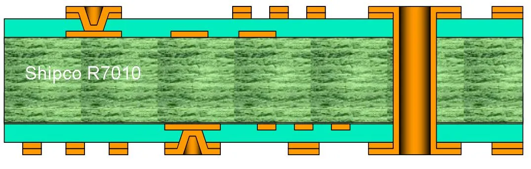
R7010 – 4-layer HDI with laser micro-vias on both sides (L1–L2 and L3–L4)
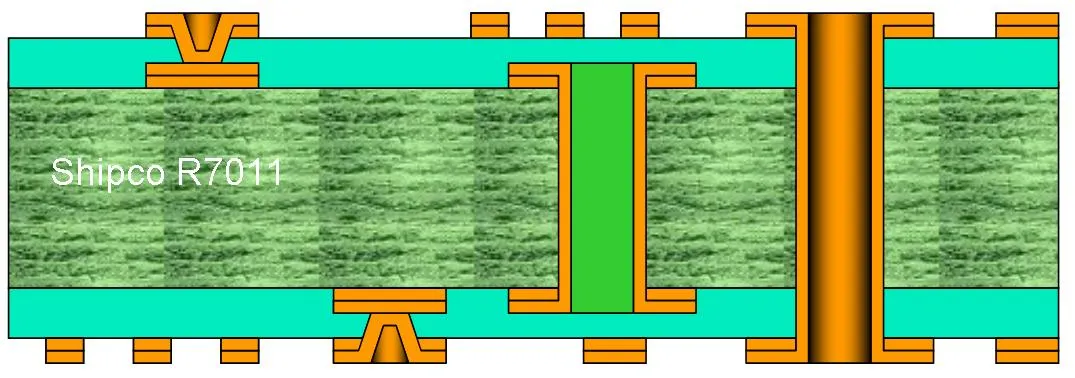
R7011 – 4-layer HDI with buried via L2–L3 and laser micro-vias L1–L2 and L3–L4
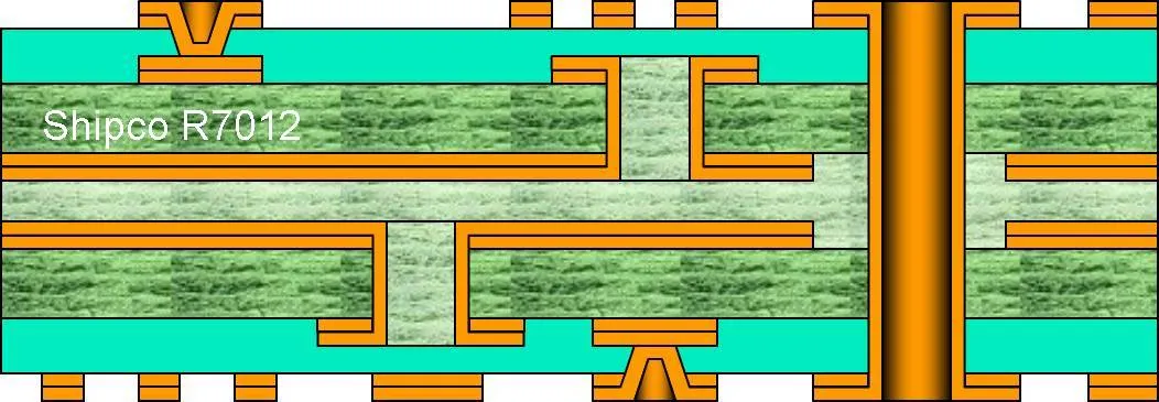
R7012 – 6-layer HDI: buried vias in core with micro-vias top and bottom (single lamination)
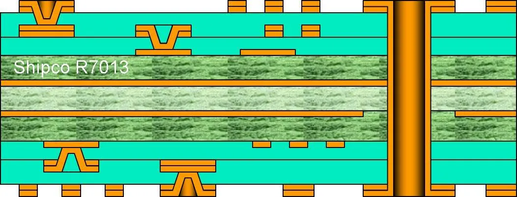
R7013 – 2+2 HDI with staggered micro-vias on both sides (two lamination stages)
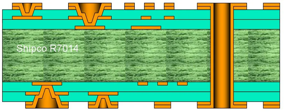
R7014 – 2+2 HDI with stacked micro-vias on both sides (two lamination stages)
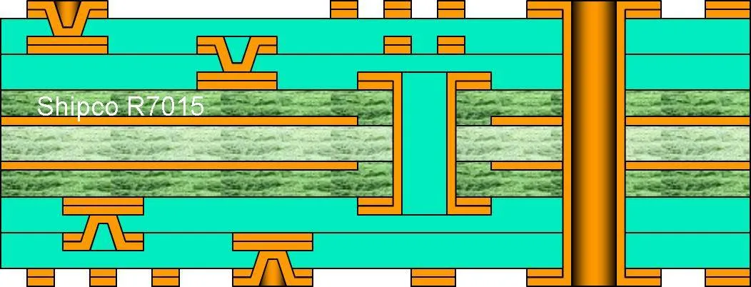
R7015 – 2+2 HDI with thin buried via (<0.8mm, no fill required) – two lamination stages
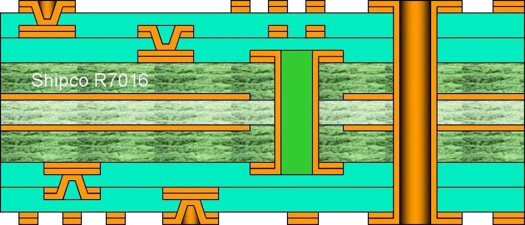
R7016 – 2+2 HDI with thick buried via (>0.8mm, requires via fill) – two lamination stages
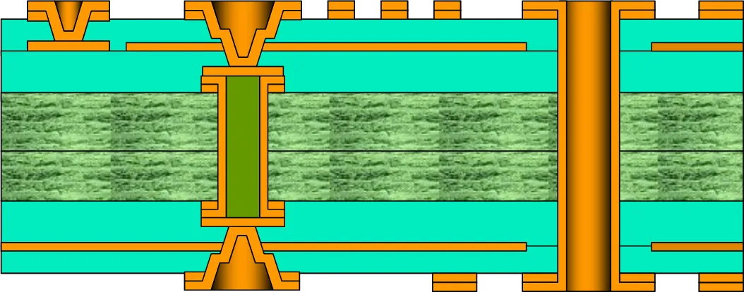
R7017 – 2+2 HDI via-in-pad: micro-via lands on filled buried via (two lamination stages)
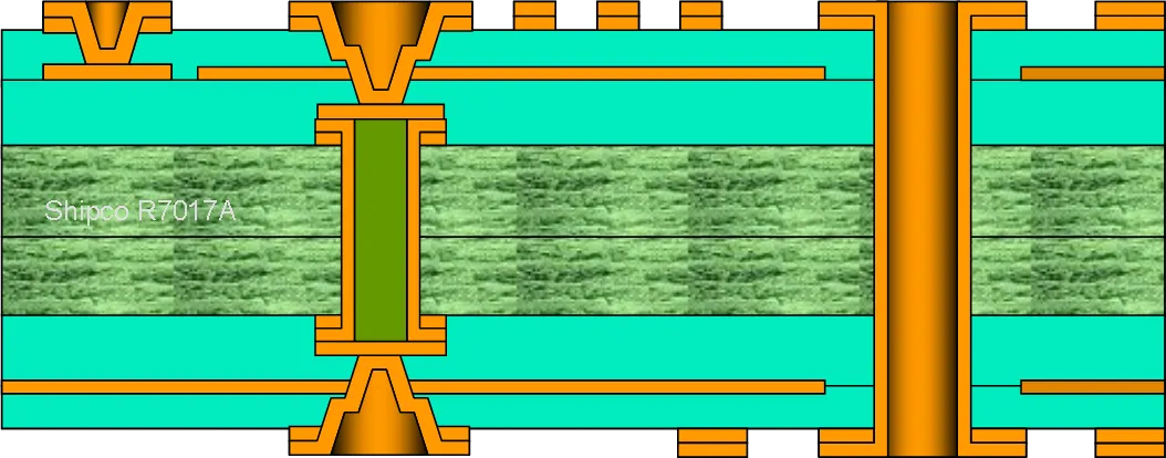
R7017A – Via-in-pad detail: micro-via stacked on copper-filled buried via
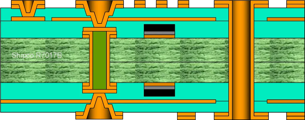
R7017B – Via-in-pad variant with embedded passives (resistors in inner layers)
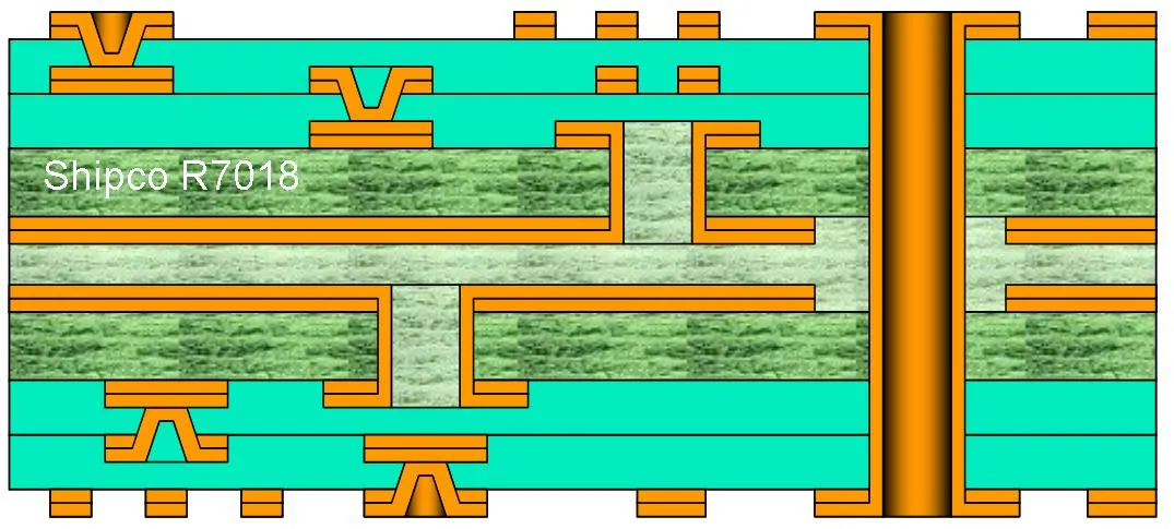
R7018 – 2+2 HDI with two buried via layers (two lamination stages)
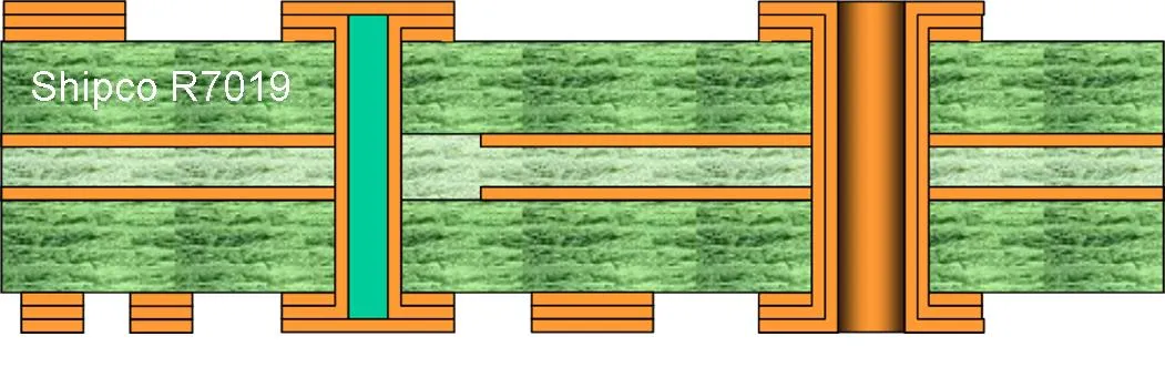
R7019 – Via-in-pad: resin-filled and flat copper over-plated (single lamination)
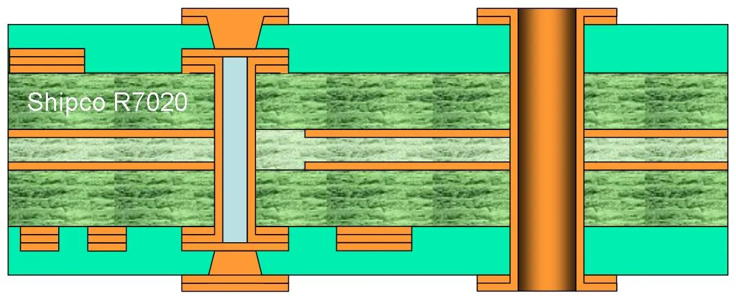
R7020 – Stacked via-in-pad: copper-filled micro-vias over buried via (two laminations)
Flex & Rigid-Flex PCB Constructions (R7021–R7024)
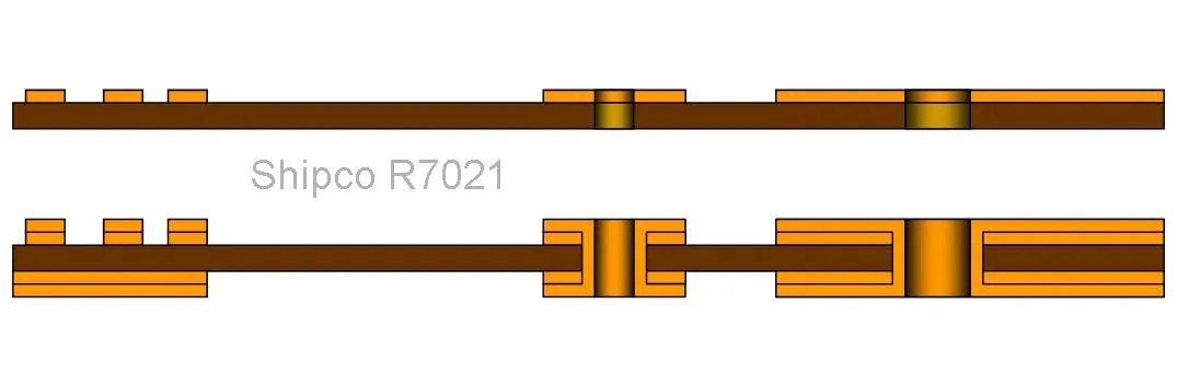
R7021 – Flex PCB comparison: single-sided NPTH (top) and double-sided PTH (bottom)
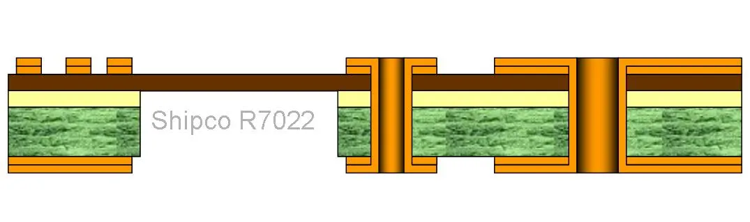
R7022 – 2-layer rigid-flex: flex polyimide core with rigid FR-4 sections (single lamination)
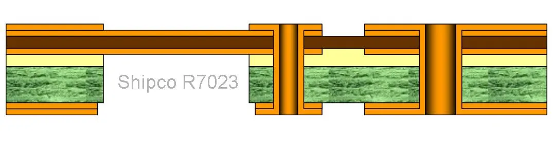
R7023 – 3-layer asymmetric rigid-flex with single flex layer (single lamination)
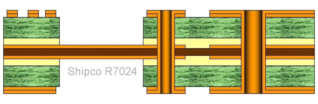
R7024 – 4-layer rigid-flex: 2-layer flex core with rigid outer layer pairs
Frequently Asked Questions
Can I use these diagrams commercially?
Yes. All illustrations on this page are free to copy and use for private, educational, or commercial purposes. No attribution required.
What do the R7000 reference codes mean?
Each code (R7001–R7024) uniquely identifies a specific PCB stackup configuration. Use these references when discussing builds with manufacturers or colleagues—they're widely recognized in the industry and searchable online.
How do I choose the right stackup for my design?
Start with the simplest build that meets your requirements. Consider layer count, via types needed for BGA breakout, impedance control requirements, and whether flex sections are necessary. When in doubt, send us your design - we review stackups at no cost and can recommend the most practical approach.
Why must PCB builds be symmetric?
Asymmetric stackups create uneven stress during lamination and thermal cycling, causing the board to warp or bow. No reputable manufacturer will produce asymmetric builds because they can't guarantee flatness—and flat boards are essential for reliable assembly.
Need help selecting a stackup?
Send us your design files or requirements. Our engineers review stackups and provide guidance at no charge—no obligation, just practical advice.
 CC BY-SA 3.0
— These PCB build illustrations are free to copy and share for private,
educational, or commercial use with attribution.
CC BY-SA 3.0
— These PCB build illustrations are free to copy and share for private,
educational, or commercial use with attribution.