

How Multilayer PCBs Are Made
Understanding PCB fabrication helps you design boards that are easier and cheaper to manufacture. A typical multilayer PCB requires around 50 process steps involving specialized equipment, precise chemistry, and careful quality control at each stage.
This guide walks through the complete fabrication process in two parts: inner layer preparation and final board production.
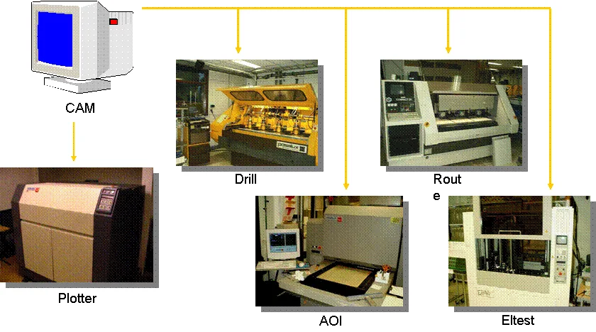
CAM station outputs data to plotters, drills, AOI, routers, and test equipment
Part 1: Inner Layer Preparation
CAM Engineering
Every PCB starts in the CAM (Computer-Aided Manufacturing) department, where your design files are prepared for production.
Input data formats accepted:
- Gerber (RS-274X)
- ODB++
- DPF, DXF, HPGL
- IPC-356 netlist
CAM preparation steps:
- Data input — Import design, drill, drawing, netlist, and specification files
- Layer definition — Assign outer layers, inner layers, solder mask, legend, and drill files
- Design rules check (DRC) — Verify against customer specs, IPC standards, and factory capabilities
- Panelization — Step PCB onto production panel with frame, tooling holes, and test coupons
- Compensation — Apply etch compensation, scaling factors, and final checks
- Output — Generate data for plotters, LDI, drill, plating, AOI, routing, and electrical test
Material Selection

Laminate inventory: different materials, thicknesses, and copper weights ready for production
Inner layer cores are selected based on your stackup requirements:
| Parameter | Common Options |
|---|---|
| Material | FR-4, High-Tg FR-4, Rogers RO4350, Teflon, Polyimide |
| Dielectric thickness | 0.1, 0.2, 0.3, 0.4mm and others |
| Copper weight | 18, 35, 70, 105μm (½oz, 1oz, 2oz, 3oz) |
Surface Pretreatment
Horizontal conveyorized pretreatment line for cleaning copper surfaces
Before imaging, copper surfaces must be:
- Cleaned — Remove oxidation, oils, and contaminants
- Micro-roughened — Create surface texture for dry film adhesion
This is done mechanically (pumice scrubbing) or chemically. The goal is a clean, oxide-free surface with consistent micro-roughness.
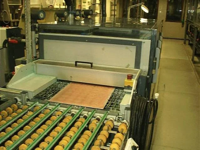
Dry Film Lamination
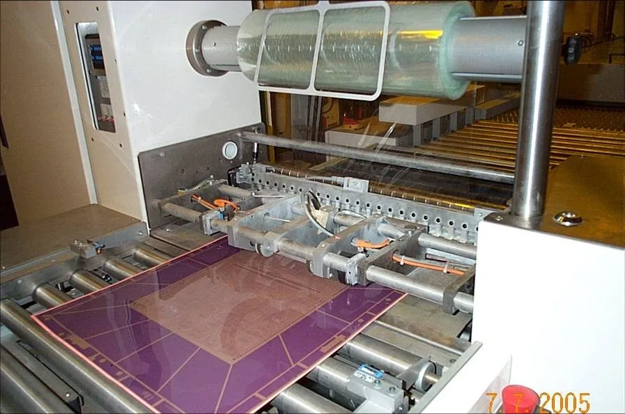
Hot roll laminator applying photosensitive dry film to copper surface
Photosensitive dry film resist is applied using heat and pressure. The film protects areas that will remain copper and exposes areas to be etched away.
Pattern Imaging
There are two methods for transferring the circuit pattern onto the dry film:
Contact Printing (Phototool)
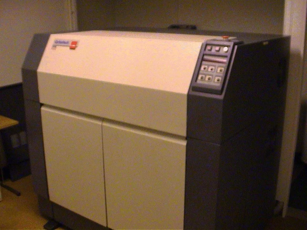
Film plotter producing silver halide phototools
Silver films are plotted and used as contact copies. UV light passes through clear areas to expose the dry film beneath.
Laser Direct Imaging (LDI)
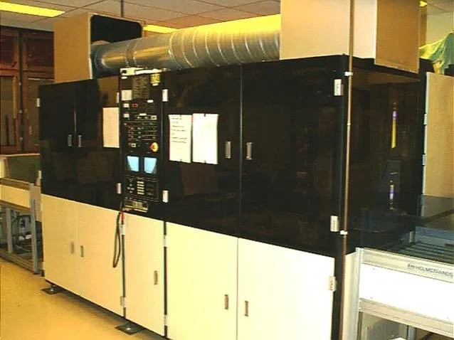
Laser Direct Imaging system for filmless exposure
LDI uses CAM data directly—no phototools required. Benefits include:
- Higher accuracy (no film distortion)
- Automatic scaling to match pre-drilled registration holes
- Faster setup for prototype and quick-turn work
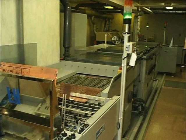
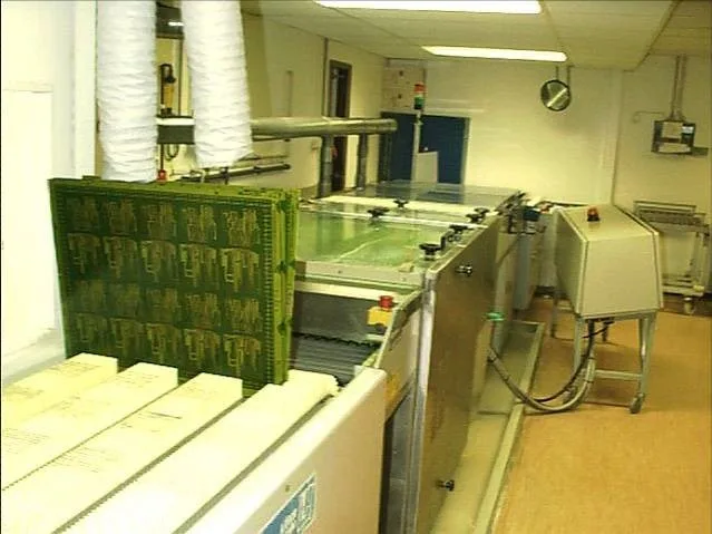
Develop, Etch, Strip (DES)
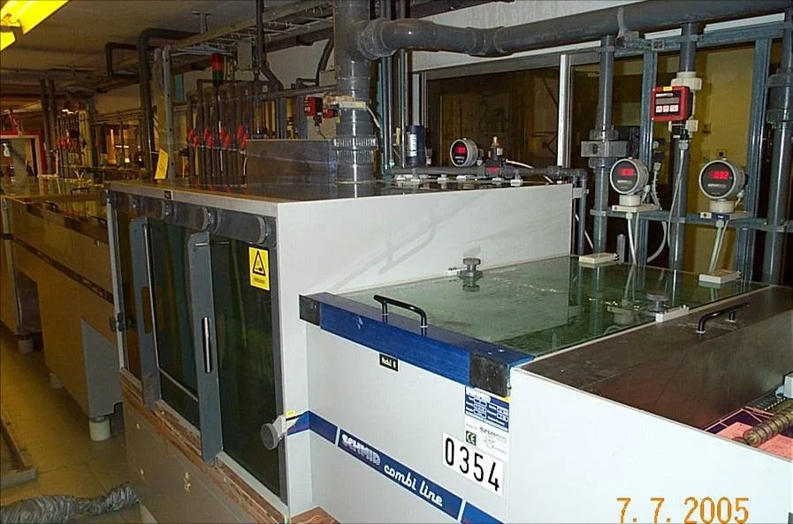
Develop-etch-strip processing line
After exposure, panels go through the DES line:
- Develop — Mild sodium carbonate solution (~1%) removes unexposed dry film
- Etch — Acidic or alkaline etchant removes exposed copper, leaving the circuit pattern
- Strip — Remaining dry film is chemically removed, revealing finished copper traces
The cross-sections below show the inner layer at each stage:
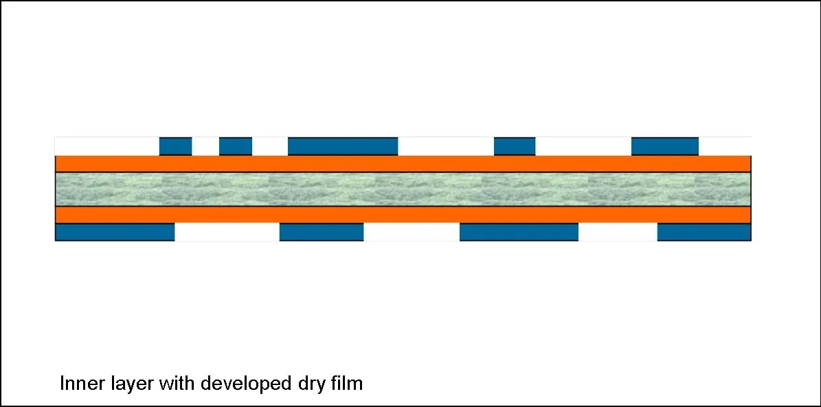
Inner layer after develop: dry film (blue) protects circuit pattern, copper exposed where it will be etched
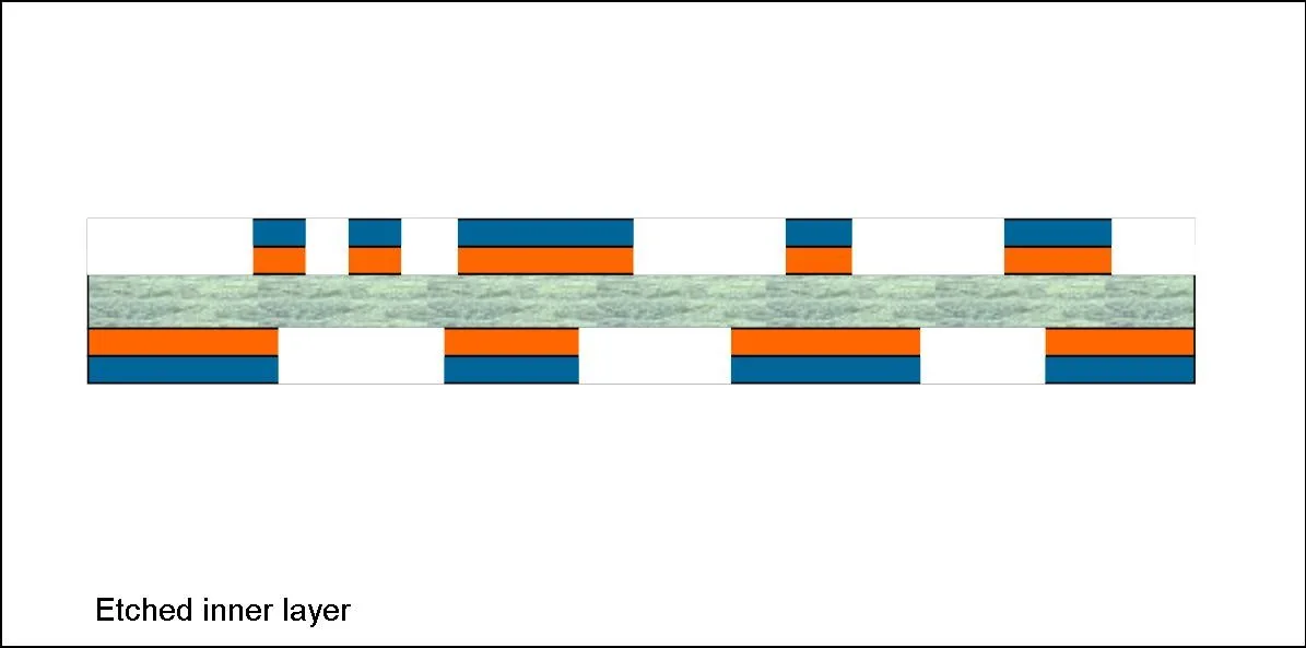
Inner layer after etch and strip: copper traces remain where protected by dry film
Automated Optical Inspection (AOI)
Every inner layer is inspected by AOI before lamination. The system:
- Compares the actual panel against CAM data
- Checks trace widths and spacing against design rules
- Identifies opens, shorts, and contamination
- Eliminates 100% of defective inner layers before they’re buried in the stackup
This is critical—inner layer defects cannot be repaired after lamination.
Layer Registration

Registration targets on inner layers must align precisely—misalignment causes drill breakout
All inner layers must align precisely when stacked. The post-etch punch:
- Uses cameras to locate targets or drilled holes on each layer
- Automatically aligns and punches registration holes
- Compensates for any material movement during processing
Layup and Lamination
Panelized inner layer ready for layup—multiple PCBs stepped on production panel
Inner layers, prepreg, and copper foil are stacked according to the stackup design:
- Layers are pinned to steel caul plates for alignment
- The stack is placed in a vacuum press
- Heat and pressure cure the prepreg resin, bonding all layers
Different materials require specific press cycles—temperature ramps, pressure profiles, and cure times are all programmed for each material system.
X-Ray Registration

Inner layer targets (circled) visible through laminate—X-ray system locates these for drilling
After pressing, material movement must be compensated. The X-ray punch:
- Sees copper targets buried inside the panel
- Calculates optimal position for new registration holes
- Ensures subsequent drilling aligns with inner layer features
Part 2: Final Board Production
For double-sided boards, production starts here. For multilayers, this continues from the laminated panel.
Drilling
Most holes are mechanically drilled at this stage:
- Standard via sizes: 0.3mm and larger
- Small holes (≤0.3mm) reduce drill stack height and increase cost
- Thick panels also limit stack height
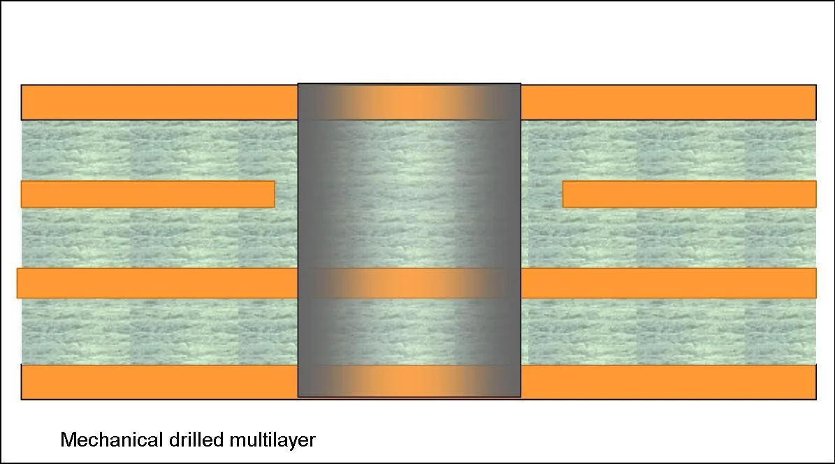
Cross-section after mechanical drilling: through-hole connects all layers, but hole walls are not yet conductive
Laser Drilling (for HDI)
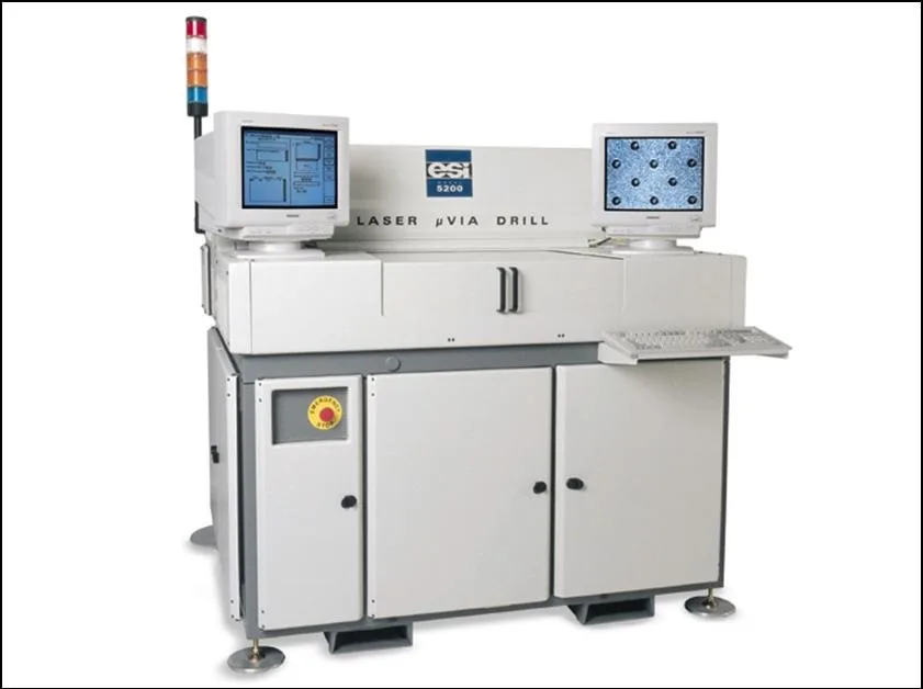
ESI 5200 UV laser drilling system for micro-vias
Micro-vias (typically 100-150μm) require laser drilling. See our micro-via advantages guide for when HDI makes sense.
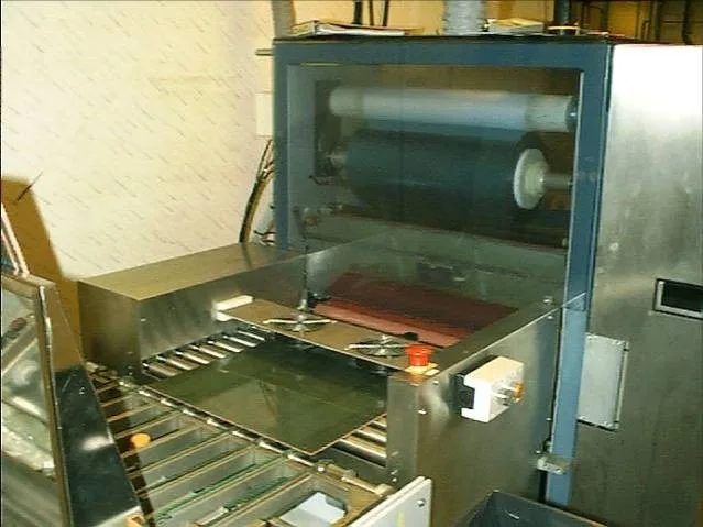
Electroless Copper Deposition
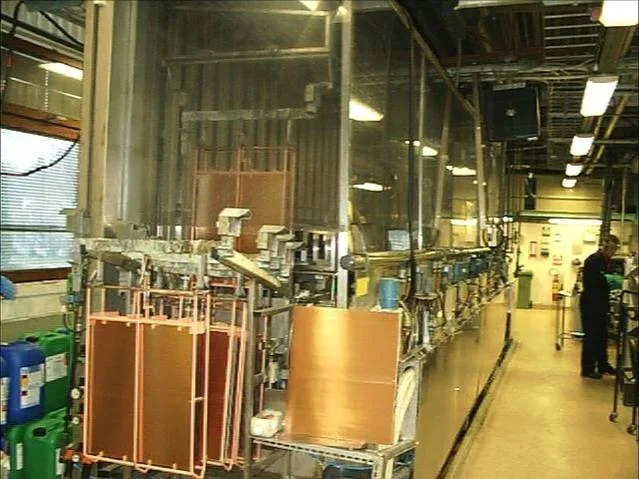
Vertical plating line—panels move through chemical baths on flight bars
This critical process deposits a thin conductive copper layer on hole walls, enabling subsequent electroplating. It involves multiple chemical baths:
- Cleaner/conditioner
- Micro-etch
- Catalyst (palladium-based)
- Electroless copper
The quality of this step determines plated through-hole reliability.
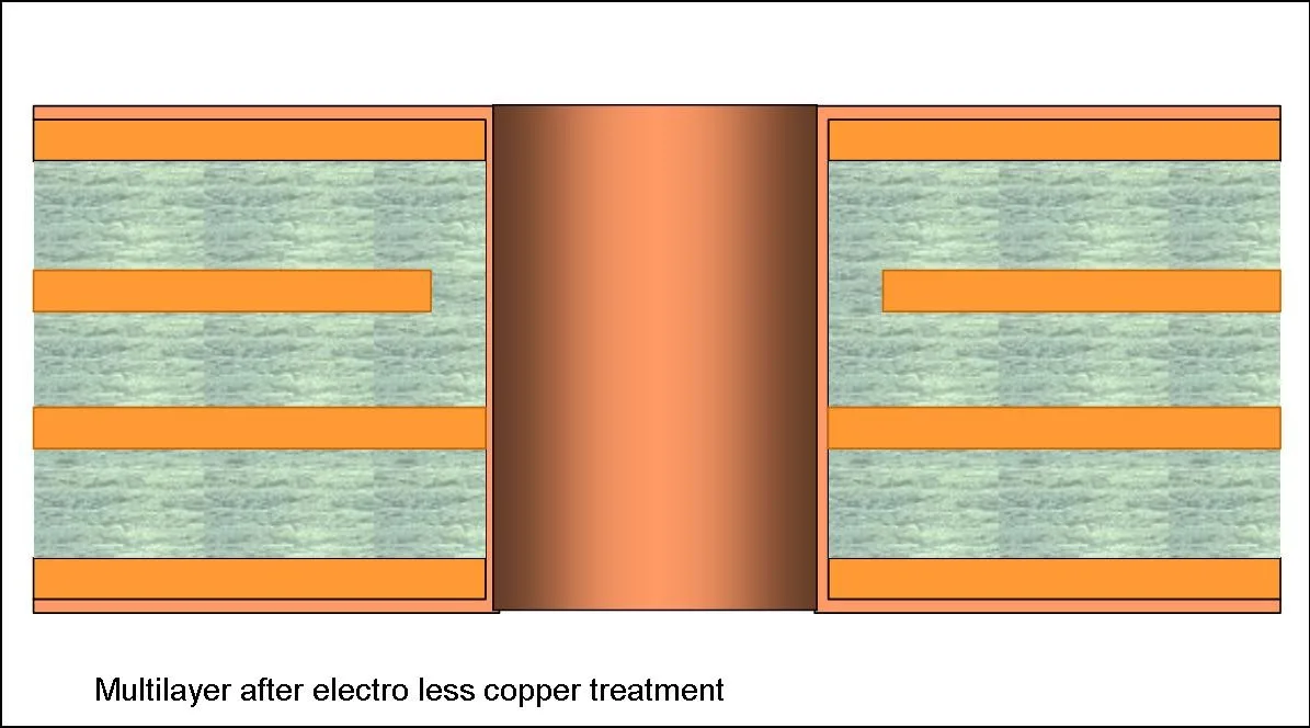
After electroless copper: thin conductive layer now coats hole walls
Outer Layer Imaging
The outer layer process mirrors inner layer imaging:
Dry film lamination for outer layers
- Laminate dry film
- Expose pattern — Contact print or LDI
- Develop — Remove unexposed resist
Pattern Plating
Unlike inner layers (which are etched from solid copper), outer layers are pattern plated:
- Electroplate copper — Build up copper in exposed areas (traces and pads)
- Electroplate tin — Etch resist to protect copper during etching
- Strip dry film — Remove photoresist
- Etch copper — Remove base copper between traces
- Strip tin — Remove tin etch resist
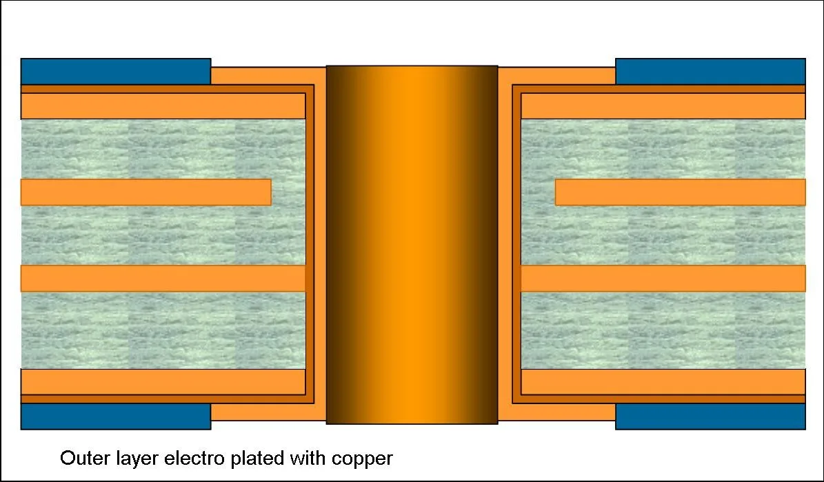
After pattern plating: copper built up on traces and in holes, dry film (blue) still in place
Outer Layer AOI
AOI inspection of outer layer patterns
Outer layers are inspected by AOI before solder mask application.
Solder Mask Application
Curtain coater applying liquid photoimageable solder mask
Solder mask protects copper from oxidation and prevents solder bridging during assembly. Application methods:
| Method | Description |
|---|---|
| Curtain coating | Liquid mask flows over panel in a curtain |
| Screen printing | Mask squeegeed through mesh screen |
| Electrostatic spray | Charged particles deposited evenly |
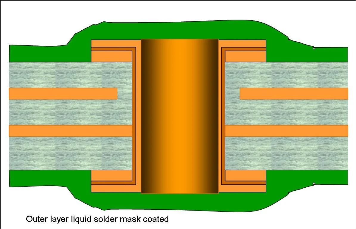
After solder mask coating: green mask covers board surface before imaging
After coating, the mask is exposed and developed like dry film, leaving openings for pads and vias.
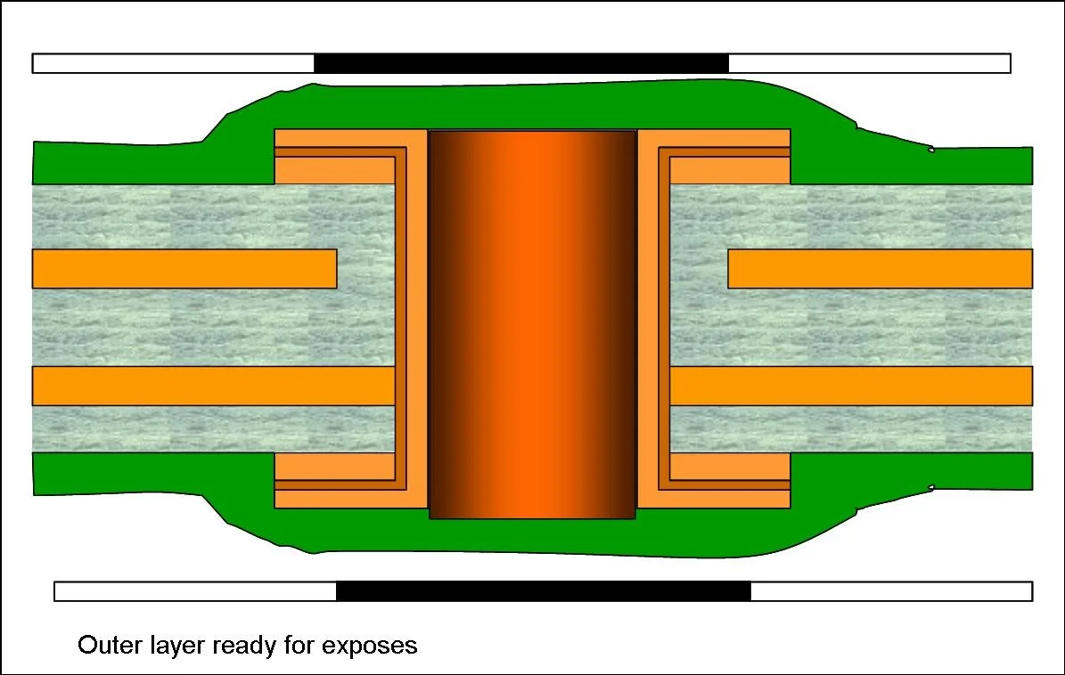
During solder mask exposure: film masks (black bars) block UV over pad areas to keep them open
Surface Finish
The exposed copper pads need protection from oxidation. Common finishes:
ENIG (Electroless Nickel / Immersion Gold)
Chemical plating line for ENIG surface finish
- Flat surface for fine-pitch BGAs
- Good shelf life
- Higher cost than HASL
Other finishes:
- HASL — Hot air solder leveling, traditional finish, excellent solderability
- OSP — Organic coating over copper, lowest cost, limited shelf life
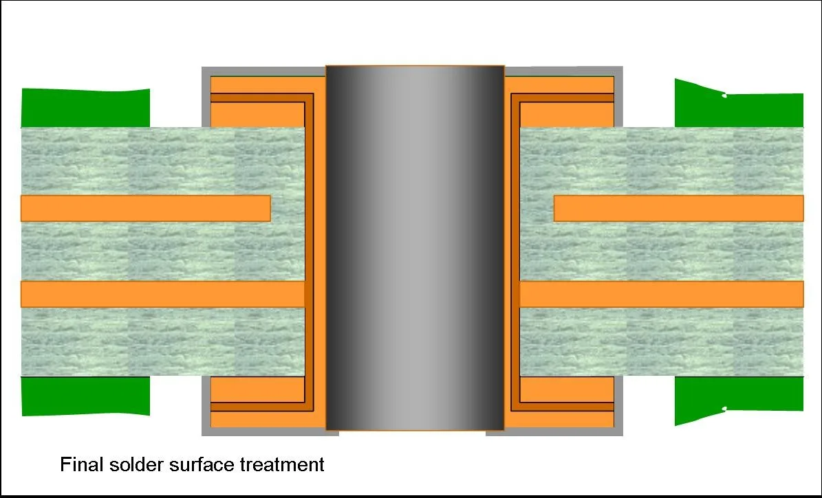
Finished board cross-section: solder mask (green) with surface finish on exposed pads
Electrical Test
Every board is electrically tested for opens and shorts.
Flying Probe Testing
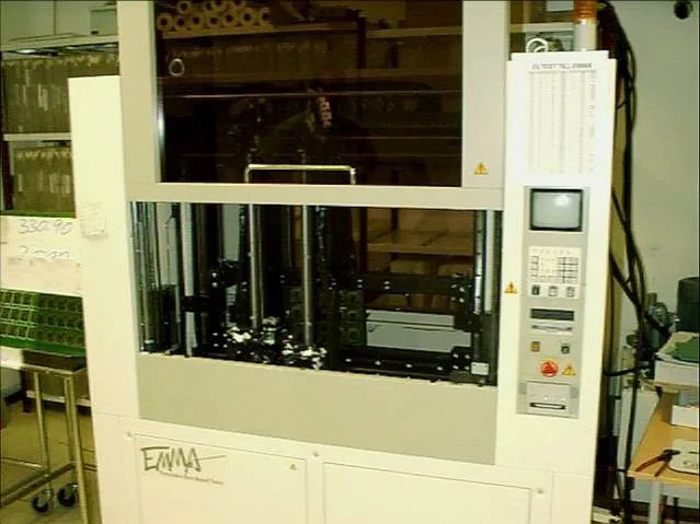
EMMA flying probe test system—probes move to test each net
- Moving probes test directly from CAM data
- No fixture required
- Ideal for prototypes and small batches
Fixture Testing
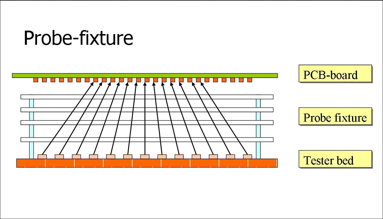
Fixture test concept: spring-loaded pins contact all test points simultaneously
- Dedicated fixture with spring-loaded pins
- Very fast for high-volume production
- Fixture fabrication adds time and cost
Routing and Scoring
Boards are separated from the production panel by:
- Routing — CNC router cuts board outline (standard: 2.4mm cutter, minimum: 0.8mm)
- Scoring — V-groove allows panels to snap apart after assembly
- Combination — Routed outlines with breakaway tabs

V-score specifications: 30° blade angle, minimum 0.4mm from score to copper, 0.2-0.35mm remaining material
Final Inspection
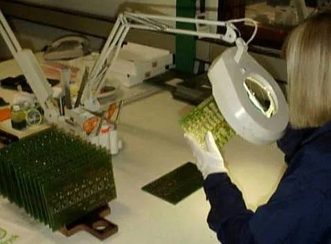
Visual inspection with magnification lamp
Final QC checks:
- Dimensional accuracy
- Surface finish quality
- Bow and twist (flatness)
- Cosmetic defects
- Compliance with specifications
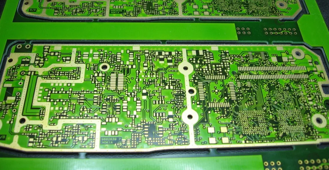
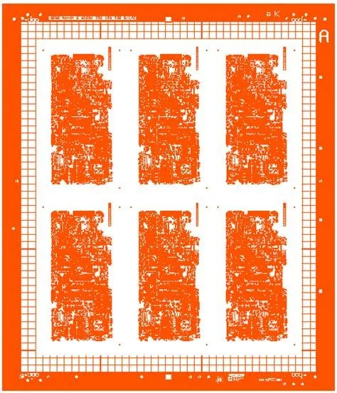
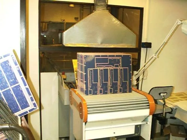
Finished PCB panel ready for shipment
Why This Matters for Your Design
Understanding fabrication helps you:
- Avoid costly design changes — Know what’s easy vs. difficult to manufacture
- Specify appropriately — Don’t over-specify tolerances you don’t need
- Communicate effectively — Use correct terminology with your manufacturer
- Troubleshoot issues — Understand root causes when problems occur
For stackup guidance, see our PCB build illustrations showing common multilayer constructions.
Questions about your design? Our engineers review manufacturability at no charge. Get in touch.