

The Problem: Heat Trapped Under Components
Power semiconductors, voltage regulators, and LED drivers generate significant heat. If that heat can’t escape through the PCB, junction temperatures rise, reliability drops, and components fail early.
Standard PCBs are poor thermal conductors—FR-4 has thermal conductivity around 0.3 W/m·K, compared to 400 W/m·K for copper. But you can dramatically improve heat transfer by adding thermal vias: dense arrays of plated through-holes that conduct heat from the component side to inner planes or the opposite surface.
How Thermal Vias Work
Plated through-holes are essentially copper tubes through the PCB. Copper’s high thermal conductivity creates a heat path through the otherwise insulating laminate.
The effectiveness depends on:
- Via density – more vias = more heat transfer
- Via diameter – larger vias have more copper area
- Plating thickness – thicker copper = lower thermal resistance
- Fill material – filled vias transfer more heat than hollow ones
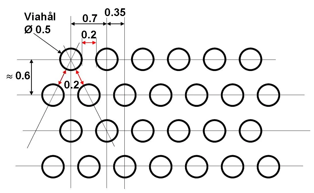
Optimal Via Pattern
For maximum thermal performance, use a staggered hex pattern:
- Drill diameter: 0.5 mm (finished ~0.4 mm after plating)
- Row pitch (X): 0.7 mm minimum (maintains 0.2 mm substrate between holes)
- Row offset (Y): 0.6 mm
- Stagger: Offset alternate rows by half the X pitch
- Repeat pitch (Y): 1.2 mm for the full pattern
Minimum copper plating: 25 µm—more is better if your process allows.
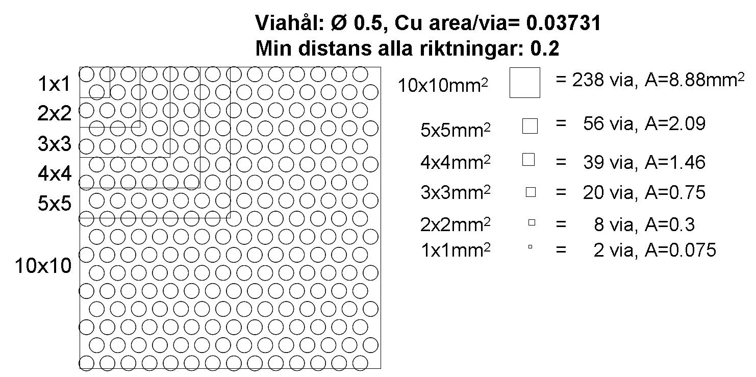
Via density comparison: tighter patterns provide more thermal transfer but increase drilling cost
Design Trade-offs
Via Size vs. Density
| Via Diameter | Pitch | Vias per cm² | Relative Thermal Performance |
|---|---|---|---|
| 0.3 mm | 0.5 mm | 400 | Highest (but expensive) |
| 0.4 mm | 0.7 mm | 200 | Good balance |
| 0.5 mm | 0.9 mm | 120 | Cost-effective |
| 0.6 mm | 1.0 mm | 100 | Standard approach |
Thermal via cross-section: plating thickness directly affects heat transfer capacity
Filled vs. Hollow Vias
- Hollow vias: Standard process, lower cost, adequate for moderate heat loads
- Filled vias: Conductive or non-conductive fill, better thermal performance, required for via-in-pad under thermal components
- Capped vias: Filled and plated over, flat surface for component mounting
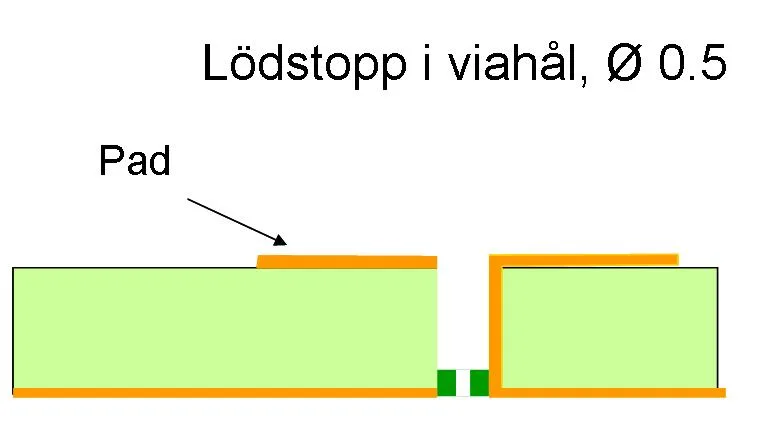
Via fill options: choose based on thermal requirements and component mounting needs
Thermal Via Placement
Under Exposed Pads
Most power components have an exposed thermal pad on the bottom. Place a dense via array directly under this pad, connecting to inner ground planes or a bottom-side heat sink area.
Connection to Planes
Thermal vias should connect to large copper areas—either inner planes or external copper pours. The plane acts as a heat spreader, distributing heat across a larger area.
Keep-Out Considerations
Don’t place thermal vias:
- Under solder paste areas (solder wicks into unfilled vias)
- Too close to signal vias (thermal cycling stress)
- Where they interfere with inner layer routing
Alternative Approaches
For extreme thermal requirements, consider:
- Metal-core PCBs (MCPCB) – aluminium or copper substrate
- Insulated metal substrate (IMS) – thin dielectric on metal base
- Embedded heat pipes – for localised hot spots
- Thick copper – 2–20 oz copper for better lateral spreading
When to Use Thermal Vias
Thermal vias are appropriate when:
- Component dissipation exceeds ~0.5 W in a small area
- Junction temperature margins are tight
- The component has an exposed thermal pad
- Standard FR-4 construction is otherwise acceptable
For detailed specifications, see the PCB Component Cooling PDF.
Related Articles
- How Multilayer PCBs Are Made – Understanding plating and drilling for thermal vias
- Multilayer PCB Capabilities – Hole size and copper weight specifications
- PCB Materials and Laminates Guide – Thermal conductivity of different materials
Need thermal management in your PCB? Request a quote – we can advise on via patterns and material selection for heat dissipation.