

The Problem: Open Vias Cause Assembly Defects
Uncovered via holes create problems during assembly. Solder wicks down into open vias, starving the joint above. Flux residue gets trapped in holes, causing reliability issues. Vacuum test fixtures can’t seal against boards with open vias. And under fine-pitch BGAs, open vias can short to adjacent balls.
The solution is controlling how solder mask interacts with your vias—and there are several options depending on your requirements.
Via Covering Options
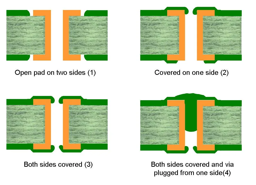
Via covering options: from fully open (left) to fully plugged (right)
1. Open Vias (No Mask)
Solder mask is pulled back from the via, leaving the hole fully exposed.
Use when:
- Via is a test point
- Intentional solder fill is required
- Via is far from components
Problems:
- Solder wicking during assembly
- Flux entrapment
- Shorts under BGAs
2. Tented Vias
Solder mask covers the via opening like a tent. The via remains hollow underneath.
Use when:
- Via is near components but not under them
- Basic protection from solder wicking is sufficient
- Lowest cost option
Limitations:
- Tent may have small holes (mask doesn’t perfectly bridge)
- Not suitable for vacuum test fixtures
- Can trap air during wave soldering
3. Plugged Vias (Mask Filled)
Via is filled with solder mask material, not just tented over.
Use when:
- Vacuum test fixtures require sealed surface
- Via is close to (but not directly under) solder paste
- Better sealing than tenting required
Process note: Fill from one side only to avoid trapping air.
4. Filled and Capped Vias
Via is filled with epoxy or conductive fill, then plated over. Results in a flat, solderable surface.
Use when:
- Via-in-pad designs (via directly in component pad)
- BGAs requiring vias under the package
- Maximum reliability and flatness required
Cost: Highest option due to additional processing steps.
Solder Mask Defined (SMD) Pads
For fine-pitch components, an alternative approach uses the solder mask to define the solderable pad area:
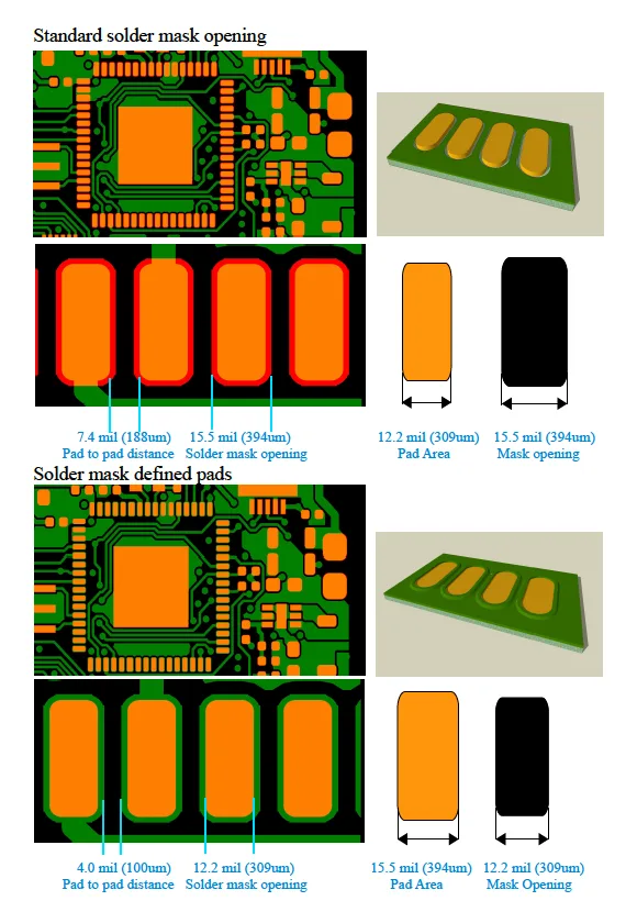
Left: Standard pad (mask opening larger than copper). Right: Solder mask defined pad (mask overlaps copper edge)
Standard Pads (NSMD)
- Solder mask opening is larger than the copper pad
- Solder fillet wraps around pad edge
- Most common approach
Solder Mask Defined Pads (SMD)
- Solder mask overlaps the pad edge
- Solder is confined to the mask opening
- Allows tighter pitch (mask controls spacing, not copper etching)
Example: 0.5 mm pitch BGA with 0.25 mm pads
- Copper pad spacing: 0.1 mm (challenging to etch reliably)
- With SMD: Copper can be larger, mask defines the 0.25 mm opening
Trade-off: SMD pads have smaller solder fillets and slightly lower joint strength, but enable finer pitches.
Design Guidelines
Under BGAs
- Never leave vias open under BGA packages
- Via-in-pad requires filled and capped vias
- Dog-bone vias (outside pad) can be tented or plugged
For Test Fixtures
- Vacuum fixtures require plugged vias (one side)
- Flying probe testing can work with any via type
Spacing Rules
| Via Treatment | Minimum Spacing to Pad |
|---|---|
| Open via | 10 mil (avoid under components) |
| Tented via | 6 mil |
| Plugged via | 4 mil |
| Filled/capped | 0 (via-in-pad allowed) |
Related Articles
- BGA Component Design Guide – BGA pad and solder mask considerations
- Multilayer PCB Capabilities – Solder mask specifications
- PCB Designer’s Tips – Design guidelines for manufacturability
Questions about solder mask options? Request a quote – we’ll recommend the best approach for your design.