

The Challenge: Routing High-Pin-Count Packages
Ball Grid Array (BGA) packages pack hundreds or thousands of connections into a small footprint. Unlike peripheral-leaded packages, BGA balls are arranged in a grid across the entire package bottom—which creates a routing challenge. You can’t simply run traces to the edge; you need to escape signals from under the package through multiple PCB layers.
Getting BGA routing right requires understanding pad geometry, via placement, and solder mask rules. Get it wrong and you’ll face assembly defects, signal integrity problems, or designs that simply can’t be manufactured.
BGA Package Structure
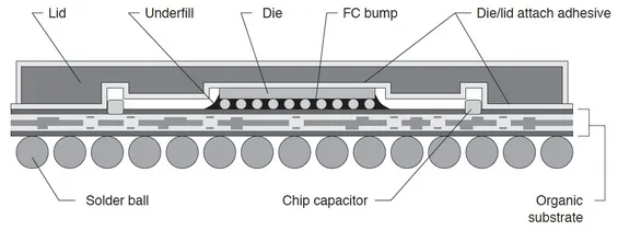
Flip chip BGA cross-section: die attached to substrate with solder balls forming the external connections
The BGA substrate routes signals from the die to the ball grid. Understanding this structure helps when debugging assembly issues or specifying package requirements.
For detailed BGA specifications, see the Texas Instruments BGA Application Guide (PDF).
Orientation and Placement
BGA orientation: pin A1 location must be clearly marked in your assembly drawing
Fanout Strategies
The key to BGA routing is the fanout pattern—how you escape signals from the ball grid to the routing layers beneath.
Dog-Bone Fanout

Dog-bone pattern: via placed adjacent to pad, connected by short trace
This is the most common approach for larger pitch BGAs (0.8 mm and above). Each pad connects to a via placed in the gap between pads.
Via-in-Pad
Via-in-pad: via drilled directly through the pad centre
For fine-pitch BGAs (0.5 mm and below), there’s no room for dog-bone fanout. The via must be placed directly in the pad, filled with conductive or non-conductive material, and planarised for reliable solder joints.
Layer Escape Patterns
Layer escape: outer rows exit on layer 1, inner rows drop to layers 2, 3, and beyond
Staggered escape pattern for dense BGAs
High-density BGA requiring four or more routing layers for full escape
Solder Mask Considerations
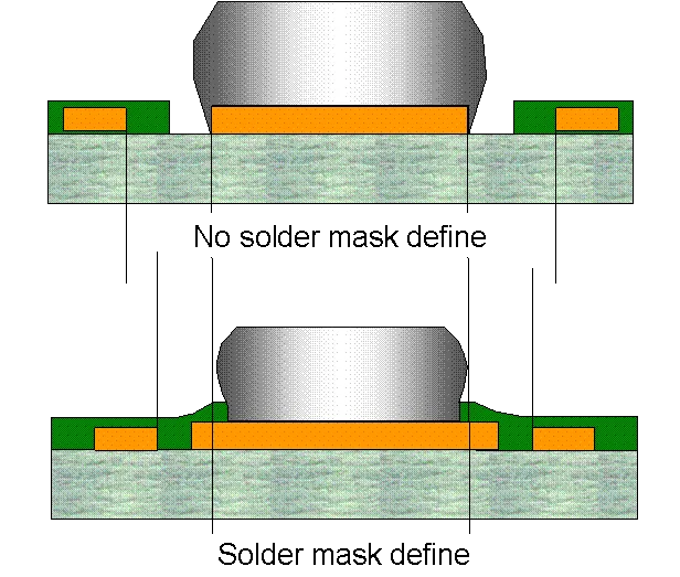
Solder mask to pad clearance: minimum 2 mil (0.05 mm) per side typical
Solder Mask Defined (SMD) vs Non-Solder Mask Defined (NSMD)
NSMD pads (most common):
- Solder mask opening is larger than the copper pad
- Better solder joint reliability—fillet forms around pad edge
- Preferred for most BGA applications
SMD pads:
- Solder mask overlaps the pad edge
- Tighter pitch capability—mask controls pad spacing
- Used when NSMD clearances can’t be achieved
Pad Size and Via Geometry
Design Parameters by Ball Pitch
All dimensions in mm:
| Ball Pitch | 1.50 | 1.27 | 1.0 | 0.80 | 0.65 | 0.50 |
|---|---|---|---|---|---|---|
| Solder Ball Diameter | 0.75 | 0.75 | 0.60 | 0.50 | 0.40 | 0.30 |
| Solder Pad Diameter | 0.50 | 0.50 | 0.40 | 0.35 | 0.30 | 0.25 |
| PTH Diameter | 0.30 | 0.30 | 0.20 | 0.20 | 0.20 | 0.15 |
| PTH Pad Diameter | 0.50 | 0.50 | 0.40 | 0.40 | 0.40 | 0.40 |
| Line Width (1 line/channel) | 0.30 | 0.25 | 0.20 | 0.125 | 0.075 | 0.075 |
| Line Width (2 lines/channel) | 0.20 | 0.15 | 0.12 | 0.075 | 0.050 | 0.050 |
Column Grid Array Routing Guidelines
Column Grid Arrays (CGAs) use solder columns instead of balls for better thermal cycling reliability. The table below shows routing parameters for standard (left columns) and fine-feature (right columns) PCB processes:
All dimensions in mm:
| Contact Pitch | 1.0 | 1.25 | 1.5 | 1.0 | 1.25 | 1.5 |
|---|---|---|---|---|---|---|
| Standard process | Fine-feature process | |||||
| Contact Land | 0.55 | 0.65 | 0.75 | 0.55 | 0.65 | 0.75 |
| Via Land | 0.61 | 0.61 | 0.61 | 0.50 | 0.50 | 0.50 |
| Via Hole | 0.33 | 0.33 | 0.33 | 0.25 | 0.25 | 0.25 |
| Annular Ring | 0.14 | 0.14 | 0.14 | 0.12 | 0.12 | 0.12 |
| Signal Line | 0.13 | 0.13 | 0.13 | 0.10 | 0.10 | 0.10 |
| Air Gap | 0.13 | 0.13 | 0.13 | 0.10 | 0.10 | 0.10 |
| Signal Tracks | 1 | 2 | 3 | 1 | 2 | 3 |
Stencil and Pad Specifications for Assembly
Solder paste stencil thickness and aperture sizing affect solder joint quality. These guidelines apply to BGA and related area-array packages:
| Component Type | Stencil Foil (mm) | Aperture Size | Board Pad |
|---|---|---|---|
| CBGA (Ceramic BGA) | 0.20 | 0.79 round | 0.71 round |
| TBGA (Tape BGA) | 0.18 | 0.81 round | 0.66 round |
| PBGA (Plastic BGA) | 0.20 | 0.79 round | 0.71 round |
| CSP (Chip Scale Package) | 0.13 | 0.36 round | 0.30 round |
Design Rules by Pitch
| BGA Pitch | Pad Diameter | Via Size | Trace Width | Routing Layers |
|---|---|---|---|---|
| 1.27 mm | 0.6 mm | 0.3 mm PTH | 6 mil | 2 (dog-bone) |
| 1.0 mm | 0.5 mm | 0.25 mm PTH | 5 mil | 2–4 |
| 0.8 mm | 0.4 mm | 0.2 mm PTH | 4 mil | 4 |
| 0.65 mm | 0.3 mm | 0.15 mm PTH | 3.5 mil | 4–6 |
| 0.5 mm | 0.25 mm | 0.1 mm laser | 3 mil | 6+ (HDI) |
| 0.4 mm | 0.2 mm | 0.1 mm laser | 2.5 mil | 6+ (HDI) |
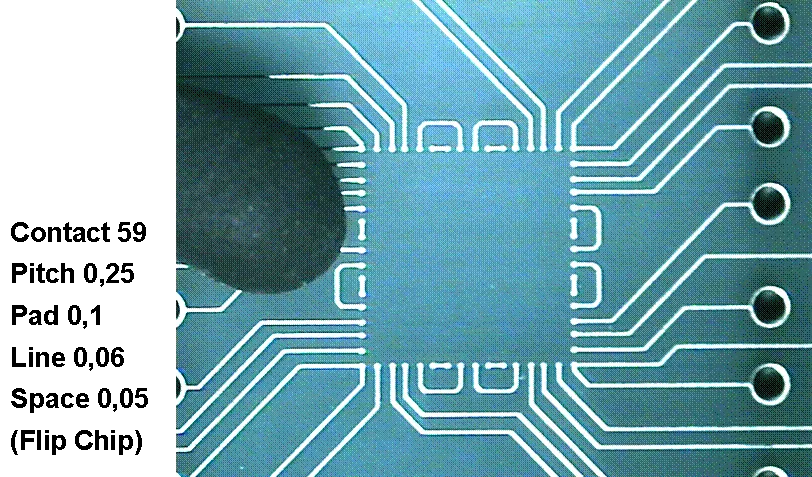
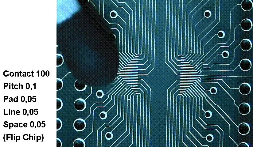
Real-World Examples
These examples show typical design parameters for production BGAs at different densities.
313-Ball BGA (1.8 mm pitch)
A large-pitch BGA routable with standard PCB processes. The wide pitch allows generous pad sizes and conventional PTH vias—no HDI required.
| Parameter | Value |
|---|---|
| Contacts | 313 |
| Pitch | 1.8 mm |
| Pad | 0.75 mm |
| Line/space | 0.15 mm |
| Vias | 0.4 mm |
| Mask opening | 0.55 mm |
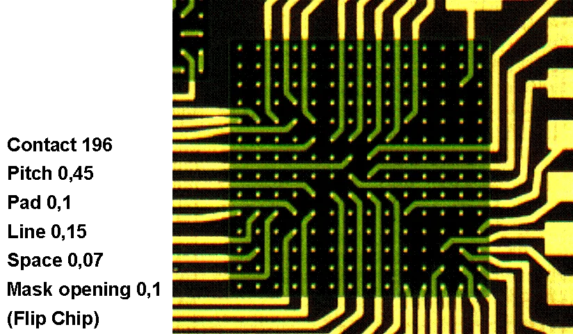
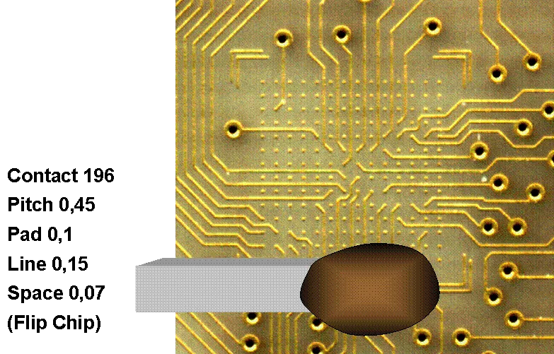
64-Ball BGA (0.8 mm pitch)
A mid-density BGA at the boundary between standard and HDI technology. Dog-bone fanout is possible but tight; micro-vias provide additional escape options.
Production BGA fanout with dog-bone via pattern
| Parameter | Value |
|---|---|
| Contacts | 64 |
| Pitch | 0.8 mm |
| Pad | 0.3 mm |
| Line/space | 0.15 mm |
| Vias | 0.3 mm |
| Micro-vias | 0.1 mm |
When HDI Is Required
Standard through-hole technology works for BGAs down to about 0.65 mm pitch. Below that, you’ll typically need HDI with micro-vias:
- 0.5 mm pitch: Usually requires 1+N+1 HDI
- 0.4 mm pitch: Often requires 2+N+2 HDI or any-layer
- Sub-0.4 mm: Almost always any-layer HDI
Related Articles
- Micro-Via Advantages in PCBs – HDI routing for fine-pitch BGAs
- Solder Mask and Via Types – Via covering options under BGAs
- Multilayer PCB Capabilities – BGA pad and routing specifications
Need help with BGA routing? Request a quote – our engineers review BGA fanout as part of every technical review.